 Engineer News Network The ultimate online news and information resource for today’s engineer
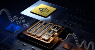
This technology is designed for use by power electronics engineers where high-power density in a small form factor is critical.
Developed in partnership with prominent power electronics designers to create a leadless multichip solution for high-efficiency and high-density power converters, KONNEKT technology utilises transient liquid phase sintering (TLPS).
These devices can be mounted to PCBs using existing reflow processes.
Capacitors utilising KONNEKT technology have the unique ability to be mounted in a low-loss orientation to further increase their power handling capability.
The first release of KONNEKT technology will combine KEMET’s ultra-stable U2J dielectric to create a low-loss, low-inductance package capable of handling very high ripple current in the hundreds of kilohertz range. KEMET will deploy this advanced RoHS compliant, 100% Pb-free technology across multiple product platforms.
“Power electronics engineers asked for a solution to help achieve higher efficiency in smaller packages,” said Dr. John Bultitude, KEMET Vice President and Technical Fellow. “KEMET’s KONNEKT technology delivers through increased efficiency by combining multiple capacitors into a single high density, ultra-low loss package.”